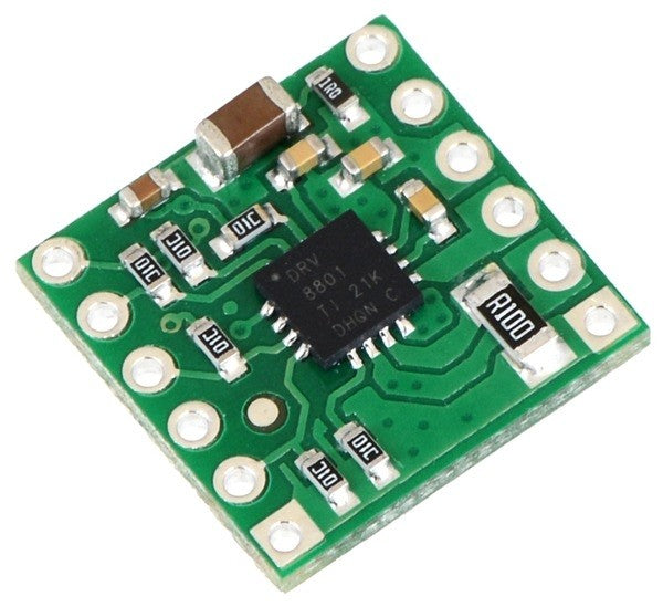
Description
Features:
- Drives a single brushed DC motor
- Motor supply voltage: 8?36 V
- Logic supply voltage: 3.3?6.5 V
- Output current: 1 A continuous (2.8 A peak)
- Simple interface requires only two I/O lines (one for direction and another for speed)
- Current sense output proportional to motor current (approx. 500 mV per A)
- Inputs are 3V- and 5V-compatible
- Under-voltage lockout and protection against over-current and over-temperature

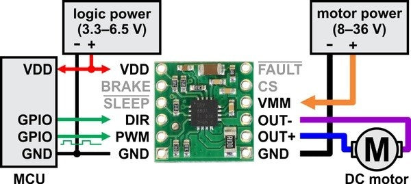
Minimal wiring diagram for connecting a microcontroller to a DRV8801 single brushed DC motor driver carrier.
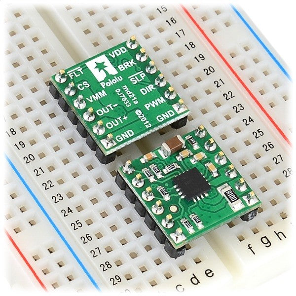
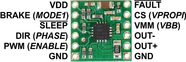
In a typical application, power connections are made on one side of the board and control connections are made on the other. Aside from motor and power connections, the only required pins are DIR and PWM (called PHASE and ENABLE in the DRV8801 datasheet, respectively). A PWM signal can be applied to the PWM/ENABLE pin to achieve variable speed control in the direction determined by the state of the DIR/PHASE pin. The carrier board pulls PWM low by default, so the driver is only enabled when this pin is supplied with a high signal. The DIR pin does not have a defined default state, which means outputs could behave erratically if the DIR pin is left disconnected while the PWM pin is high.
The BRAKE pin determines whether the motor brakes or coasts when PWM pin is low (this pin is called MODE1 in the DRV8801 datasheet). The carrier board pulls it high, which corresponds to braking (both motor outputs are shorted together through ground). Setting the BRAKE pin low sets the outputs to coast whenever the PWM pin is low (both motor outputs are off). We generally recommend leaving this high while supplying a PWM signal to the PWM pin to get drive-brake (or ?slow-decay?) operation, as this typically provides a more linear relationship between PWM duty cycle and motor speed than drive-coast (or ?fast-decay?), and it can result in better performance at low duty cycles. The following truth table shows how the PWM, DIR, and BRAKE pins affect the driver outputs:
| DRV8801 Truth Table | |||||
|---|---|---|---|---|---|
| PWM/ENABLE | DIR/PHASE | BRAKE/MODE1 | OUT+ | OUT- | operating mode |
| PWM | 1 | 1 | PWM (H/L) | L | forward/brake at speed PWM % |
| PWM | 0 | 1 | L | PWM (H/L) | reverse/brake at speed PWM % |
| L | X | 1 | L | L | brake low (outputs shorted to ground) |
| PWM | 1 | 0 | PWM (H/OPEN) | PWM (L/OPEN) | forward/coast at speed PWM % |
| PWM | 0 | 0 | PWM (L/OPEN) | PWM (H/OPEN) | reverse/coast at speed PWM % |
| L | X | 0 | OPEN | OPEN | coast (outputs off) |
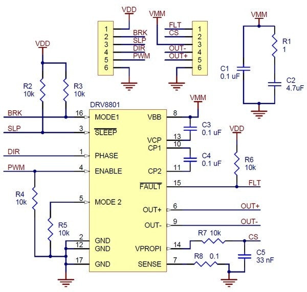
The SLEEP pin is pulled high on the board through a 10k resistor and can be left disconnected if you do not want to use the low-power sleep mode of the DRV8801.
The FAULT pin is an open-drain output that is driven low by the chip whenever an over-current, over-temperature, or under-voltage condition occurs. The carrier board includes a pull-up resistor on this pin, so no external pull-up is necessary. Note that the FAULT pin is a status-only signal that does not affect device functionality, so a low FAULT signal does not necessarily mean the driver outputs are disabled. For example, the driver will start operating normally once the motor supply voltage is above 8 V, but the FAULT output will be low until the motor supply voltage reaches approximately 12 V. Please see the datasheet for more information about how the DRV8801 responds to and reports faults.
The CS pin outputs an analog voltage proportional to the motor current (approximately 500 mV per A).
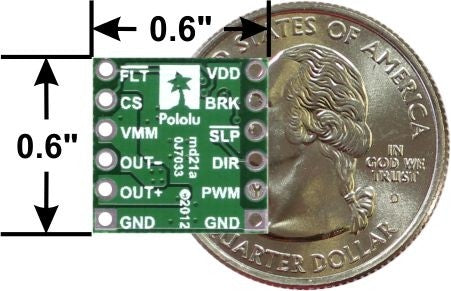
Pinout:

|
PIN |
Default State |
Description |
|
VMM/VBB |
|
8?36 V motor power supply connection. This pin called VBB in the DRV8801 datasheet. |
|
VDD |
|
3.3?6.5 V logic power supply connection. This pin is only used to power theFAULT, SLEEP, and BRAKE pull-up resistors on the carrier board. (The DRV8801 has its own internal logic voltage regulator.) |
|
GND |
|
Ground connection points for the motor and logic power supplies. The control source and the motor driver must share a common ground. |
|
OUT+ |
|
H-bridge output +. |
|
OUT- |
|
H-bridge output -. |
|
DIR/PHASE |
undefined |
Logic input for controlling motor direction. |
|
PWM/ENABLE |
LOW |
Logic input for enabling the driver outputs/controlling motor speed. A PWM signal can be applied to this pin. |
|
BRAKE/MODE1 |
HIGH |
Logic input for controlling whether the driver brakes low or coasts when PWM pin is low. A logic high results in braking (slow-decay through ground). |
|
SLEEP |
HIGH |
Logic input that puts the DRV8801 into a low-power sleep mode when low. |
|
FAULT |
|
Logic output that drives low when a fault occurs. The carrier board pulls this pin up to VDD. |
|
CS/VPROPI |
|
Analog voltage output proportional to motor current (500 mV per A). |
This product can get hot enough to burn you long before the chip overheats. Take care when handling this product and other components connected to it.
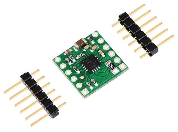
Included hardware:


Schematic:

Dimensions:
- Size: 0.6? × 0.6?1
- Weight: 0.7 g1
- Motor driver: DRV8801
- Motor channels: 1
- Minimum operating voltage: 8.0 V
- Maximum operating voltage: 36 V
- Continuous output current per channel: 1 A2
- Peak output current per channel: 2.8 A
- Current sense: 0.5 V/A
- Reverse voltage protection?: N
- 1.Without included hardware.
- 2.Typical results with 100% duty cycle at room temperature.
Encrypted payment
Your payment information is processed securely. We do not store credit card details nor have access to your credit card information.
Customs tariff number:
Country of origin:
This depends on where you are located. Once the order has been handed over to UPS, the delivery time in Germany is approx. 2-3 days, within Europe approx. 1 week.
We dispatch our articles with our shipping partner UPS.
If we have not yet answered your question, you can contact us and we will get back to you as soon as possible.

